ESP32 DEVKIT V1 — GPIO Reference
A lookup table for the 30‑pin ESP‑WROOM‑32 board: pick a pin without breaking booting or Wi‑Fi.
Rule of thumb: for a plain input or output, reach for a ✅ safe pin first — GPIO 4, 13, 16, 17, 18, 19, 21, 22, 23, 25, 26, 27, 32, 33.
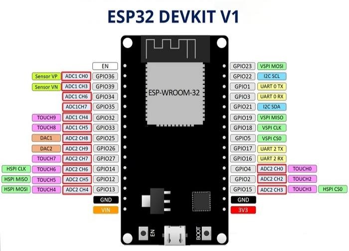
1 · Quick categories
| Category | Pins | Why |
|---|---|---|
| SAFE general‑purpose | 4, 13, 16, 17, 18, 19, 21, 22, 23, 25, 26, 27, 32, 33 | Use these first for I/O |
| STRAPPING (read at boot) | 0, 2, 5, 12, 15 | Usable, but a wrong level can block uploading |
| BOOT HIGH/PWM | 1, 3, 5, 14, 15 | May glitch attached outputs at reset |
| INPUT‑ONLY | 34, 35, 36 (VP), 39 (VN) | No output, no internal pull |
| DO NOT USE (flash) | 6, 7, 8, 9, 10, 11 | Wired to the SPI flash — not broken out |
| 🔌 USB serial | 1 (TX0), 3 (RX0) | Used by the Serial Monitor — avoid for I/O |
2 · Full pin table
I = input · O = output · ADC = analog‑in · Touch = capacitive touch · DAC = analog‑out.
| GPIO | Label | I | O | ADC | Touch | Other | Notes |
|---|---|---|---|---|---|---|---|
| 36 | VP | ✅ | — | ADC1_CH0 | — | Sensor VP | input only |
| 39 | VN | ✅ | — | ADC1_CH3 | — | Sensor VN | input only |
| 34 | D34 | ✅ | — | ADC1_CH6 | — | — | input only |
| 35 | D35 | ✅ | — | ADC1_CH7 | — | — | input only |
| 32 | D32 | ✅ | ✅ | ADC1_CH4 | T9 | — | safe |
| 33 | D33 | ✅ | ✅ | ADC1_CH5 | T8 | — | safe |
| 25 | D25 | ✅ | ✅ | ADC2_CH8 | — | DAC1 | safe |
| 26 | D26 | ✅ | ✅ | ADC2_CH9 | — | DAC2 | safe |
| 27 | D27 | ✅ | ✅ | ADC2_CH7 | T7 | — | safe |
| 14 | D14 | ✅ | ✅ | ADC2_CH6 | T6 | HSPI CLK | PWM at boot |
| 12 | D12 | ✅ | ✅ | ADC2_CH5 | T5 | HSPI MISO | strapping boot fails if pulled HIGH |
| 13 | D13 | ✅ | ✅ | ADC2_CH4 | T4 | HSPI MOSI | safe |
| 23 | D23 | ✅ | ✅ | — | — | VSPI MOSI | safe |
| 22 | D22 | ✅ | ✅ | — | — | I²C SCL | safe |
| 21 | D21 | ✅ | ✅ | — | — | I²C SDA | safe |
| 19 | D19 | ✅ | ✅ | — | — | VSPI MISO | safe |
| 18 | D18 | ✅ | ✅ | — | — | VSPI CLK | safe |
| 5 | D5 | ✅ | ✅ | — | — | VSPI CS | strapping HIGH at boot; PWM at boot |
| 17 | TX2 | ✅ | ✅ | — | — | UART2 TX | safe |
| 16 | RX2 | ✅ | ✅ | — | — | UART2 RX | safe |
| 4 | D4 | ✅ | ✅ | ADC2_CH0 | T0 | — | safe |
| 2 | D2 | ✅ | ✅ | ADC2_CH2 | T2 | On‑board LED | strapping floating/LOW to flash |
| 15 | D15 | ✅ | ✅ | ADC2_CH3 | T3 | HSPI CS | strapping HIGH at boot; PWM at boot |
| 1 | TX0 | — | ✅ | — | — | UART0 TX | Debug output at boot — avoid |
| 3 | RX0 | ✅ | — | — | — | UART0 RX | HIGH at boot — avoid |
| 0 | (BOOT) | ✅ | ✅ | ADC2_CH1 | T1 | Boot select | strapping tied to BOOT; not on header |
Pins 6–11 connect to the module's SPI flash and are not exposed — never use them.
3 · Peripheral defaults
| Bus | Signal → pin |
|---|---|
| I²C | SDA = GPIO 21, SCL = GPIO 22 (reassignable in code) |
| SPI — VSPI | MOSI 23 · MISO 19 · CLK 18 · CS 5 |
| SPI — HSPI | MOSI 13 · MISO 12 · CLK 14 · CS 15 |
| UART0 (USB Serial) | TX 1 · RX 3 |
| UART2 | TX 17 · RX 16 |
| DAC (analog out) | DAC1 = 25 · DAC2 = 26 |
4 · ADC & touch
ADC is 12‑bit → readings 0–4095 for 0–3.3 V.
- ADC1 (always usable): GPIO 32, 33, 34, 35, 36, 39
- ADC2 (⚠️ unusable while Wi‑Fi is on): GPIO 0, 2, 4, 12, 13, 14, 15, 25, 26, 27
Touch T0–T9: T0=4, T1=0, T2=2, T3=15, T4=13, T5=12, T6=14, T7=27, T8=33, T9=32.
5 · Electrical limits
- ≤ 40 mA per GPIO absolute; keep ≤ ~12 mA in practice.
- Logic is 3.3 V — never apply 5 V to a GPIO.
- Input‑only pins (34/35/36/39) have no internal pull — add an external resistor for buttons.